| Sign In | Join Free | My chinacomputerparts.com |
|
| Sign In | Join Free | My chinacomputerparts.com |
|
| Categories | RF PCB Board |
|---|---|
| Brand Name: | Bicheng |
| Model Number: | BIC-332.V1.0 |
| Certification: | UL, ISO9001, IATF16949 |
| Place of Origin: | CHINA |
| MOQ: | 1PCS |
| Price: | USD9.99-99.99 |
| Payment Terms: | T/T |
| Supply Ability: | 5000PCS per month |
| Delivery Time: | 8-9 working days |
| Packaging Details: | Vacuum bags+Cartons |
| PCB material: | RF-10 |
| PCB thickness: | 0.5mm |
| Layer count: | 2-layer |
| PCB size: | 143.6mm x 109.8mm (2 Types, 2 PCS) |
| Copper weight: | 1oz (1.4 mils) on outer layers (35μm) |
| Surface finish: | ENEPIG |
| Company Info. |
| Bicheng Electronics Technology Co., Ltd |
| Verified Supplier |
| View Contact Details |
| Product List |
Looking for a high-performance 2-layer rigid PCB optimized for RF applications? This 2-layer rigid PCB is built with RF-10 copper clad laminates—a composite of ceramic-filled PTFE and woven fiberglass—designed to address the growing need for size reduction in RF applications while maintaining superior signal integrity. Engineered to IPC-Class 2 quality standards, this PCB delivers reliable performance for critical applications like microstrip patch antennas, GPS antennas, and satellite components. With a focus on precision, durability, and cost-effectiveness, this PCB is ideal for engineers and procurement teams seeking a reliable substrate for high-frequency projects.
PCB Specifications
Every aspect of our PCB is engineered for precision and performance, ensuring consistency and reliability in every unit:
| Construction Item | Details |
| Board Dimensions | 143.6mm x 109.8mm (2 Types, 2 PCS), with a tight tolerance of +/- 0.15mm for precise fit in your assemblies |
| Trace & Space | Minimum 5/7 mils, enabling compact circuit design without compromising signal integrity |
| Minimum Hole Size | 0.4mm, compatible with standard component mounting requirements |
| Vias | No blind vias, simplifying manufacturing while ensuring reliable interlayer connections |
| Finished Board Thickness | 0.5mm, balancing durability and space efficiency for compact devices |
| Copper Weight | 1oz (1.4 mils) on outer layers (35μm), providing excellent conductivity for high-frequency signals |
| Via Plating Thickness | 20μm, meeting IPC-Class 2 standards for reliable electrical connections and mechanical strength |
| Surface Finish | ENEPIG, offering superior solderability, corrosion resistance, and compatibility with modern assembly techniques compared to standard finishes like ENIG |
| Silkscreen & Solder Mask | No top or bottom silkscreen, no top or bottom solder mask, ensuring a clean design optimized for RF signal performance |
| Quality Testing | 100% electrical test performed prior to shipment, guaranteeing functionality and eliminating defective units |
PCB Stack-up Configuration
| Stack-up Component | Specifications & Description |
| Copper Layer 1 | 35μm (1oz) – Ensures efficient signal transmission and thermal conductivity |
| RF-10 Core | 10mil (0.254mm) – The foundation of the PCB’s superior RF performance |
| Copper Layer 2 | 35μm (1oz) – Provides consistent conductivity and symmetry for balanced signal flow |
PCB Statistics
| PCB Statistics Item | Details & Description |
| Components | 24 – Accommodates essential components for RF circuits |
| Total Pads | 51 – Provides ample connectivity options |
| Thru Hole Pads | 34 – Supports reliable through-hole component mounting |
| Top SMT Pads | 17 – Enables surface-mount component integration on the top layer |
| Bottom SMT Pads | 0 – Optimized for specific component layouts |
| Vias | 29 – Ensures secure interlayer connections |
| Nets | 2 – Simplifies circuit routing while maintaining signal integrity |
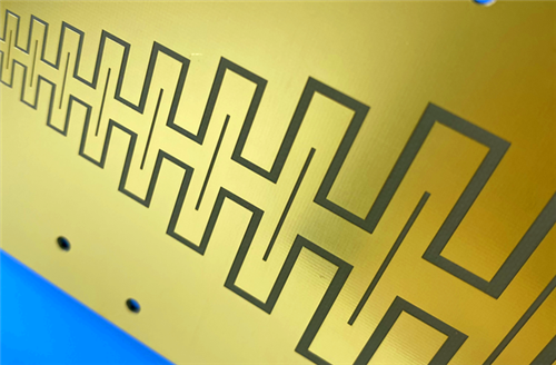
RF-10 Substrate: Key to Superior Performance
RF-10 copper clad laminates are the cornerstone of our PCB’s exceptional performance, engineered to meet the demands of high-frequency RF applications:
RF-10 is a composite of ceramic-filled PTFE and woven fiberglass, offering a unique combination of high dielectric constant (DK) and low dissipation factor—critical for reducing signal loss at higher frequencies. The thin woven fiberglass reinforcement enhances rigidity for easier handling and improved dimensional stability, making it ideal for both single-layer and multilayer circuits.
Engineered for cost-effectiveness and industry-acceptable delivery times, RF-10 addresses the need for size reduction in RF applications. Its excellent bonding with smooth low-profile copper, combined with low dissipation, results in optimal insertion losses at higher frequencies where skin effect losses are significant.
Key Features of RF-10 PCB
Our RF-10 2-layer PCB boasts industry-leading features that set it apart for high-frequency applications:
Dielectric Constant: 10.2 ± 0.3 at 10GHz – Enables compact RF circuit design
Dissipation Factor: 0.0025 at 10GHz – Minimizes signal loss for reliable high-frequency performance
High Thermal Conductivity: 0.85 W/mk (Unclad) – Enhances thermal management, preventing overheating in high-power applications
CTE (Coefficient of Thermal Expansion): x=16 ppm/°C, y=20 ppm/°C, z=25 ppm/°C – Low expansion across all axes for excellent dimensional stability
Low Moisture Absorption: 0.08% – Ensures reliability in humid environments
Flammability Rating: V-0 – Meets safety standards for electronic devices
Benefits of Choosing RF-10 PCB
RF-10 PCB delivers tangible advantages for engineers, manufacturers, and procurement teams:
High DK for RF Circuit Size Reduction – Reduces the footprint of your RF designs without sacrificing performance
Excellent Dimensional Stability – Ensures consistent performance across temperature changes and manufacturing processes
Tight DK Tolerance (10.2 +/- 0.3) – Guarantees consistency across all PCBs, simplifying design and assembly
High Thermal Conductivity – Enhances thermal management, extending the lifespan of your devices
Excellent Adhesion to Smooth Coppers – Ensures reliable component bonding and signal transmission
Low X, Y, Z Expansion – Reduces the risk of solder joint failure and board warping
Excellent Price/Performance Ratio – Delivers high-quality RF performance at a cost-effective price point
Applications
Our RF-10 2-layer PCB is specifically designed for high-frequency and high-reliability applications, including:
Quality & Availability
Quality Standard: IPC-Class 2 – Meets the industry’s most common quality requirements for dedicated service electronic products, ensuring reliable performance and extended lifespan. IPC-Class 2 is widely used for communication devices, industrial instruments, and other applications requiring consistent performance.
Artwork Format: Gerber RS-274-X – The industry-standard format for PCB manufacturing, ensuring compatibility with all major design and fabrication software.
Availability: Worldwide – We offer global shipping to meet the needs of engineers and manufacturers around the globe, with industry-acceptable delivery times.


|
 RO4003C Ultimate PCB High Frequency Material For RF Microwave Applications
Rogers RO3003 High Frequency PCB 2-Layer Rogers 3003 10mil Circuit Board DK3.0 DF 0.001 Microwave PCB
RO3035 20mil 0.508mm DK3.5 RF PCB Board For Direct Broadcast Satellites
1.6mm TLF-35 RF PCB Board Ultra Low Moisture Absorption Rate
RF-35TC 0.8mm RF PCB Board
RO3010 25mil 0.635mm Microwave PCB Board LPSM Solder Mask
Rogers RO3006 High Frequency Printed Circuit Board 2-Layer Rogers 3006 10mil PCB DK6.15 DF 0.002 Microwave Gold PCB
60mil AD250C Double Sided Rigid Circuit Board With Hot Air Soldering Level
TP1020 PCB Double-layer 4mm Thick ENIG Finish
30mil Dual Layer RF PCB Based On AD300D Substrate With Immersion Silver
RO4003C Ultimate PCB High Frequency Material For RF Microwave Applications
Rogers RO3003 High Frequency PCB 2-Layer Rogers 3003 10mil Circuit Board DK3.0 DF 0.001 Microwave PCB
RO3035 20mil 0.508mm DK3.5 RF PCB Board For Direct Broadcast Satellites
1.6mm TLF-35 RF PCB Board Ultra Low Moisture Absorption Rate
RF-35TC 0.8mm RF PCB Board
RO3010 25mil 0.635mm Microwave PCB Board LPSM Solder Mask
Rogers RO3006 High Frequency Printed Circuit Board 2-Layer Rogers 3006 10mil PCB DK6.15 DF 0.002 Microwave Gold PCB
60mil AD250C Double Sided Rigid Circuit Board With Hot Air Soldering Level
TP1020 PCB Double-layer 4mm Thick ENIG Finish
30mil Dual Layer RF PCB Based On AD300D Substrate With Immersion Silver

