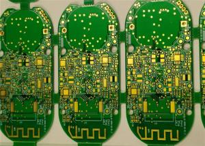
4 Layer BGA Rigid FR4 PCB , Blind Hole Circuit Board Fabrication

|
4 Layer BGA Rigid FR4 PCB , Blind Hole Circuit Board Fabrication Quick detail: Surface: Lead free HASL Layer number:4 Special technology:blind hole Hole:PTH Origin:China Model:XCEF Specification PCB Type: multilayer PCB Layer : 4 layer Min .Line Width/......
Shenzhen Xinchenger Electronic Co.,Ltd
|
Fanyi PCB blind and buried via fr4 multilayer pcb circuit board

|
...PCB blind and buried via fr4 multilayer pcb circuit board 1. Product Description Item Specification PCB type Rigid PCB, FPC, Rigid-Flex PCB Min panel size 50*50mm Max Panel size 450*450mm Surface control Lead, Lead free, Kapton Tape,DIP,Automatic coating of three defenses BGA pitch 0.35mm PCB......
Shenzhen Fany Technology Co.,Ltd
|
Meidearpcb,Multilayer PCB,Blind&Buried Vias PCB,Advanced Technology Printed Circuit Boards

|
Meidearpcb,Multilayer PCB,Blind&Buried Vias PCB,Advanced Technology Printed Circuit Boards .box_meidear { text-align:center; width:800px; margin:0 auto; font-size:......
Shenzhen Meidear Co., Limited
|
10 Layers Communication PCB Blind Via PCB With HASL Lead Free 230 * 550 Mm

|
10 Layers Blind Vias Communication PCB Board Circuit with HASL Lead Free Blind vias is designed in this PCB board. The aperture of blind via is 0.1 mm. And the Min. Line width / spacing are 0.08 / 0.05mm. This PCB is designed to used in communication ......
Shenzhen Lefang Electronics Co., Ltd
|
Rigid 1.6mm Four Layer Pcb Blind And Buried Vias

|
... ,rigid-flex pcb ,aluminum pcb ,high frequency board ,blind and buried vias and DHI Board . HDI PCB Board is the High-Density Interconnect (HDI) Printed Circuit Boards. There is little space between the PCB components, making the board space smaller, at...
Beijing Haina Lean Technology Co., Ltd
|
4 Layer Half Hole PCB Finished Thickness 0.8MM / Hdi Pcb Blind And Buried Holes

|
...Blind And Buried Holes 4 Layer Half Hole Printed Circuit Board With Blind And Buried Holes PCB Specifications: Layer Count: 4Layer Half Plated Hole PCB Board Thickness: 0.8MM Copper Thickness: 1/H/H/1OZ BGA Size: 10 Mil, Via In Pad Min Hole: 0.1MM Min Line: 3/3 Mil Hole: L1-L4 Blind......
Witgain Technology Ltd
|
10 Layer Rigid Flex Pcb Prototype Polyimide Multilayer Pcb Blind Hole

|
10 Layer Blind Hole Rigid-Flex Multilayer PCB The 10 Layer Blind Hole Rigid-Flex Multilayer PCB is a kind of Rigid-Flex Printed Circuit Board developed and produced by Shenzhen Quanhong Electronics Co., Ltd. It is manufactured by DuPont + Shengyi s1000-2m ......
Quanhong FASTPCB
|
4 Layer HDI PCB Blind Buried Holes 1.6 MM Thickness TG 150 Material

|
... Lind Space&Width: 6/6mil 6 Copper Thickness: 1/1/1/1 OZ 7 Application Area: Consumer Products 8 File Format: Gerber File 9 PCB Size: 110mm*100mm/6pcs 10 Other Requirements: 0.2MM Holes on BGA PAD, Need to do epoxy filled in...
Witgain Technology Limited
|
12-Layer BGA PCB, HDI PCB Blind via, Buried via Multi-layer PCB, High density interconnection PCB, Via and its function

|
Why do we need to use via in PCB? And its Parasitic Capacitance and Parasitic Inductance Tag# PCB design, Multi-layer PCB, High density interconnection PCB PCB holes Via is one of the important parts of multi-layer PCB, and the cost of drilling usually ......
Shenzhen Bicheng Electronics Technology Co., Ltd
|
FR4 Material 3layer 2OZ 2U'' HASL/ENIG surface green/blue soldermask HDI Pcb Blind Holes Impedance Control BGA

|
PCB board Layer: 4-16 Material: FR4 laminate, RoHS Directive-compliant PCB thickness: 0.4-6.0mm Final copper: 0.5-6oz Min hole: 0.1mm Min line width/space: 3/3 mil Min hole copper: 20/25µm Solder masks: green/blue/red/black/gray/white Legend: white/black/......
ShenZhen KaiZhuo Electronic Technology Co.,Ltd
|
