| Sign In | Join Free | My chinacomputerparts.com | 
 | 
| Categories | Fused Silica Wafer | 
|---|---|
| Brand Name: | BonTek | 
| Model Number: | Fused Silica, Fused Quartz | 
| Certification: | ISO:9001, ISO:14001 | 
| Place of Origin: | China | 
| MOQ: | 5 pcs | 
| Price: | Negotiable | 
| Payment Terms: | T/T | 
| Supply Ability: | 20000 pcs/Month | 
| Delivery Time: | 1-4 weeks | 
| Packaging Details: | Cassette/ Jar package, vaccum sealed | 
| Material: | Borosilicate Glass | 
| Glass: | Pyrex BF33 | 
| Brand: | Schott Brand | 
| Use: | Anodic Bonding, MEMS | 
| Diameter: | 100mm, 150mm, 200mm,etc. | 
| Thickness: | 0.5mm, 1mm, etc. | 
| Edge: | Round Ground Bevel | 
| Surface Type: | Single / Double Side Polish | 
| Company Info. | 
| Hangzhou Freqcontrol Electronic Technology Ltd. | 
| Verified Supplier | 
| View Contact Details | 
| Product List | 
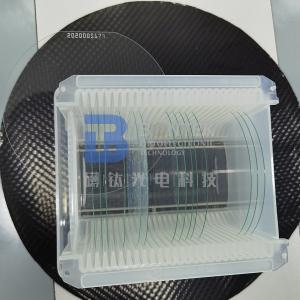
High Chemical Resistance Borosilicate Glass Wafer 4'' 6'' 8'' for MEMS Devices
Glass wafers made of borosilicate glass are often used in Semiconductor and MEMS industry in a wide variety of applications. These wafers can be used for the encapsulation of MEMS devices for example for sensors using Wafer-Level-Packaging (WLP) technology or as blank glass substrates for semiconductor processing and optics.
The borosilicate glass wafers BonTek fabricated have a coefficient of thermal expansion (CTE) that is adapted to silicon, which makes them the perfect substrate to use in anodic bonding. The glass features good transmission over a wide spectrum as well as high chemical resistance and mechanical strength. Furthermore, these wafers can be used in high temperature processing.
| Spec | 4" | 6" | 8" | 
| Diameter | 100mm | 150mm | 200mm | 
| Thickness | 0.10mm up | 0.30mm up | 0.40mm up | 
| Primary Flat | 32.5mm | 47.5mm / 57.5mm / Semi-Notch | Semi-Notch | 
| LTV (5mmx5mm) | < 0.5um | < 0.5um | < 0.5um | 
| TTV | < 2um | < 3um | <3um | 
| Bow | ±20um | ±30um | ±40um | 
| Warp | ≤ 30um | ≤ 40um | ≤ 70um | 
| Edge Rounding | Compliant with SEMI M1.2 Standard/refer to IEC62276 | ||
| Surface Type | Single Side Polished / Double Sides Polished | ||
| Polished side Ra | Ra≤1nm | ||
| Back Side Criteria | Ra 0.2-0.7um or Customized | ||


| Material | PYREX BF33 | 
| Density | 2.23 g/cm3 | 
| Modulus of Elasticity | 63 kN/mm2 | 
| Knoop Hardness HK 0.1/20 | 480 | 
| Poisson’s Ratio | 0.2 | 
| Dielectric Constant (@ 1 MHz & 25°C) | 4.6 | 
| Loss Tangent (@ 1 MHz & 25°C) | 37 x 10-4 | 
| Dielectric Strength(@ 50 Hz & 25°C) | 16 kV/mm | 
| Refractive Index | 1.472 | 
| Dispersion (nF - nC) | 71.9 x 10⁻⁴ | 


FAQs:
A: We look at ourselves as the piezo wafer specialist. We are the very first to work with Single Crystal Quartz in China about 30 years ago. Then gradually we step in the field of LiNbO3, LiTaO3, Quartz glass, LGS, CTGS etc. Especially, if you are looking for a piezo quartz supplier, we are the ultimate choice! We export millions of quartz blanks each year because we master the AT, SC and IT cuts with superior angle precision.
A: Yes, of course. We can fabricate as per your request. In addition, we are so experienced with piezo wafers that we can provide you relevant suggestions if you are not 100% sure about your choice. Besides, we do have some standard wafers in stock, please check with us.
A: Yes, we would suggest you go with the courier agent you are most familiar with (DHL, FedEX, UPS etc.). We can ship via your account. And, of course, we will pack the products safely in acceptable size to help you save the shipping cost. If you need us to take care of the freight, it’s also not a problem. We also have good discount with the international courier companies.
A: The wafer products are fragile and sometimes expensive. The last thing, as the manufacturer, we want to see is the products we make were damaged during courier. As a result, we will pack the wafers adequately and put them in a proper carton filled with buffer sponge. However, accidents are inevitable sometimes. So, please follow the “Acceptance check” steps shown in the drawings below. If the unwanted happened, we will either give the replenishment or refund if you follow the checking steps.
A: Sure. Factory inspection is important for large quantity purchase and long-term cooperation. Face to face discussion is what we mostly confident with. During the past years, big names around the world have witnessed our progress in factory build-up. These days, due to the Covid-19 pandemic, we also had the experience of videoconferencing with global buyers.
Acceptance Check

|   | 
 4'' 6'' Fused Silica Wafer 500um SiO2 HPFS with Excellent Chemical Resistance


                                                            4'' 6'' Fused Silica Wafer 500um SiO2 HPFS with Excellent Chemical Resistance
                                                    
                        
                     4 Inch 6 Inch 0.5mm Borofloat 33 Glass Wafer For Biotechnology Microelectronics


                                                            4 Inch 6 Inch 0.5mm Borofloat 33 Glass Wafer For Biotechnology Microelectronics
                                                    
                        
                     Semiconductor Use Fused Silica Wafer With Low CTE For UV Lithography


                                                            Semiconductor Use Fused Silica Wafer With Low CTE For UV Lithography
                                                    
                        
                     4 Inch 100mm SiO2 Fused Silica Wafer Corning 7980 For Immediate Shipment


                                                            4 Inch 100mm SiO2 Fused Silica Wafer Corning 7980 For Immediate Shipment
                                                    
                        
                     Customized Square Shape Borofloat 33 Glass Substrate With A Wide Range Of Uses


                                                            Customized Square Shape Borofloat 33 Glass Substrate With A Wide Range Of Uses
                                                    
                        
                     Synthetic Quartz Fused Silica Wafer Double Side Polish 4inch 0.5mm Thick


                                                            Synthetic Quartz Fused Silica Wafer Double Side Polish 4inch 0.5mm Thick
                                                    
                        
                     JGS1 JGS2 JGS3 Fused Silica Wafer and BF33 C7980 BK7 H-K9L Glass Wafers


                                                            JGS1 JGS2 JGS3 Fused Silica Wafer and BF33 C7980 BK7 H-K9L Glass Wafers
                                                    
                        
                     0.5mm 1mm Glass Carrier Wafer Customized for MEMS and Semiconductor


                                                            0.5mm 1mm Glass Carrier Wafer Customized for MEMS and Semiconductor
                                                    
                        
                     150mm 200mm Fused Silica Wafer Borosilicate With Flat Or Notch Edge Ground


                                                            150mm 200mm Fused Silica Wafer Borosilicate With Flat Or Notch Edge Ground
                                                    
                        
                     Diameter 150mm Glass Wafers Thickness 0.35mm in Fused Silica Borosilicate


                                                            Diameter 150mm Glass Wafers Thickness 0.35mm in Fused Silica Borosilicate