| Sign In | Join Free | My chinacomputerparts.com |
|
| Sign In | Join Free | My chinacomputerparts.com |
|
| Categories | HDI PCB Board |
|---|---|
| Brand Name: | WITGAIN PCB |
| Model Number: | P10E3589A0 |
| Certification: | UL Certificate |
| Place of Origin: | China |
| MOQ: | negotiable |
| Price: | negotiable |
| Payment Terms: | T/T |
| Supply Ability: | 1kkpcs/month |
| Delivery Time: | 25 work days |
| Packaging Details: | 40pcs/bag, 20bags/carton |
| Material: | FR4, TG170 |
| Board Thickness: | 1.0MM |
| Solder Mask: | Green |
| Min Hole: | 0.1MM |
| Min Trace: | 3/3Mil |
| BGA: | 7 Mil |
| Surface Treatment: | Immersion Gold |
| Company Info. |
| Witgain Technology Ltd |
| View Contact Details |
| Product List |
10 Layer HDI Printed Circuit Board , PCB Board , Green Solder Mask , ENIG
PCB Specifications:
Layer Count: 10 Layer HDI PCB
Board Thickness: 1.6MM
Material: FR4 High TG
Min Hole: 0.1MM
Min Line: 3/3 Mil
BGA: 7Mil
Hole: L1-L2, L2-L3, L3-L8, L8-L9, L9-10, L1-L10
Solder Mask: Green
Surface Treatment: ENIG
Application: Consumer Electronics
Capabilities:
| Item | Capability |
| Layer Count | 1-24 Layers |
| Board Thickness | 0.1mm-6.0mm |
| Finished Board Max Size | 700mm* 800mm |
| Finished Board Thickness Tolerance | +/-10% +/-0.1(<1.0mm) |
| Warp | <0.7% |
| Major CCL Brand | KB/NanYa/LTEQ/ShengYi/Rogers Etc |
| Material Type | FR4,CEM-1,CEM-3,Aluminum,Copper,Ceramic, PI, PET |
| Drill Hole Diameter | 0.1mm-6.5mm |
| Out Layer Copper Thickness | 1/20Z-8OZ ; |
| Inner Layer Copper Thickness | 1/3OZ-6OZ |
| Aspect Ratio | 10:1 |
| PTH Hole Tolerance | +/-3mil |
| NPTH Hole Tolerance | +/-1mil |
| Copper Thickness Of PTH Wall | >10mil(25um) |
| Line Width And Space | 2/2mil |
| Min Solder Mask Bridge | 2.5mil |
| Solder Mask Alignment Tolerance | +/-2mil |
| Dimension Tolerance | +/-4mil |
| Max Gold Thickness | 200u'(0.2mil) |
| Thermal Shock | 288C, 10s, 3 Times |
| Impedance Contro | +/-10% |
| LTest Capability | PAD Size Min 0.1mm |
| Min BGA | 7mil |
| Surface Treatment | OSP, ENIG, HASL, Plating Gold, Carbon Oil,Peelable |
FAQ:
Questions: How many lamination times for this 10 Layer HDI PCB?
Answer: For this PCB, there are 3 times lamination in total.
Questions: What is the normal lead time for this kind of PCB?
Answer: The standard lead time for sample is about 3 weeks, for production is about 4 weeks. It may fluctuate according to production and orders status.
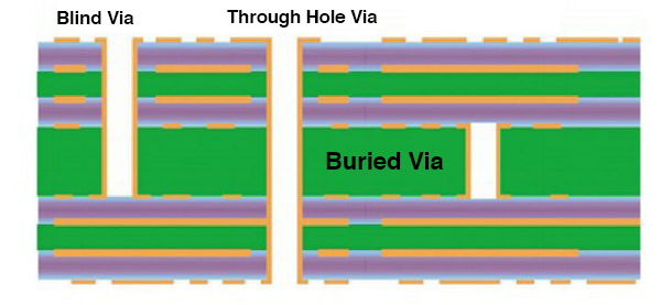
Questions: What is Blind Vias/Blind Holes?
Answer: Blind Vias connect the outermost layer of a multilayer PCB to a layer in the middle of the board. Blind vias can only be seen on one side of the board (that's where they get the name from). These vias enable designers to optimize their circuit layout by providing more space for routing. However, in comparison to Through-Hole Vias they are more difficult to construct and can cause the cost of constructing of the PCB to rise.

Questions: What Is Buried Vias/Buried Holes?
Anwer: A Buried Via hole connects layers inside a multi-layer PCB. These vias cannot be seen on the surface of a Printed Circuit Board. Buried vias are difficult to construct, as they need to be created in layers within the PCB. Designers like to use these vias, as they do not take up board space on every layer, thereby enabling smaller PCBs. High-density PCBs use buried vias.


|